IRIS (Infra-Purple, in situ) Mission Updates « bunnie’s weblog

A objective of mine is to offer on a regular basis folks tangible causes to belief their {hardware}. Betrusted is a multi-year challenge of mine to ship a full-stack verifiable “from logic gates to Rust crates” provide chain for security-critical purposes corresponding to password managers. At this level, many elements of the challenge have come collectively: Precursor is an FPGA-based open {hardware} implementation, and it runs Xous, our Rust-based microkernel message-passing OS. I at the moment use my Precursor each day with the “vault” software loaded to handle my passwords, TOTP tokens, and FIDO/U2F logins.
Nevertheless, Precursor is dear, as a result of FPGAs are costly. The system might be less expensive with a devoted safety chip, however then we have now no cause to belief these chips – safety chip distributors don’t facilitate any type of user-side inspection, so we will’t inform if we have now actual or pretend safety chips in our system.
Form of defeats the aim, for those who ask me.
Final March, I launched the idea of Infra-Purple, in situ (IRIS) inspection of silicon in a blog post and an arXiv paper. My hope has been that IRIS, plus some circuit-level scans and mathematical strategies, might be the lacking hyperlink that permits us to transition from our costly FPGA-based Precursor answer, to a extra pocketbook-friendly ASIC-based answer.
On the time after I launched the preliminary paper, each image was manually composed and targeted; each sharp picture was cherry-picked from dozens of fuzzy photographs. It was troublesome to breed photographs, and unsuitable for robotically tiling a number of photographs collectively. The method was adequate for a demo, however shaky as a basis for full-chip verification.
Over the previous yr, I’ve refined the method and applied a totally automated system that may robustly and repeatably picture entire chips at micron-scale decision in a matter of minutes. The thought just isn’t for everybody to have certainly one of these robots of their dwelling (however how cool would that be!); quite, the concept is that the majority customers may make the most of a cheap however considerably fiddly setup and evaluate their outcomes in opposition to reference photographs generated by the few customers like me who’ve totally automated techniques.
Right here’s an instance of the MPW7 run on SKY130A, courtesy of Matt Venn, imaged utilizing my automated IRIS machine:
The above is only a thumbnail; click on on the picture to zoom into and browse the full-resolution model at siliconpr0n.org (and take a look at my collection on that server for some extra full-chip IRIS photographs). Every of the mottled dots within the lighter-shaded rectangles within the picture corresponds to a logic gate, flip flop, or a “fill cell” (dummy transistors wired up as decoupling capacitors). To create the picture, I simply needed to inform the machine the place three corners of the chip are, and it robotically focuses and scans the complete space. A script then post-processes the tiles into the fully-composed picture you see right here.
A broad objective of the challenge is to democratize silicon imaging and enhance the cutting-edge in {hardware} verification. That is an space the place merely popularizing silicon imaging can transfer the needle on safety for everybody, as a result of a reputable risk of being caught reduces the inducement for adversaries to spend money on costly Trojan-implantation capabilities.
The excellent news is that the challenge is now at a state the place, over the subsequent couple of months, I can share a sequence of posts that element the methodology used to develop the automated IRIS system, in addition to doc the development of the system.
To kick issues off, I’m going to begin with a evaluate of the present cutting-edge in {hardware} verification.
Evaluation: Present State of the Artwork in {Hardware} Verification
Is my laptop reliable? How do I do know it was constructed accurately, and can execute my directions faithfully? These are the questions that {hardware} verification goals to reply.
{Hardware} verification occurs at each degree of the availability chain. Let’s begin with the relatable, every-day drawback of how do I choose a chunk of {hardware} to purchase, and from there dive all the way in which right down to esoteric subjects corresponding to verifying the circuits and gadgets that make up the {hardware} itself.

Customers searching for a pc rely principally on repute mechanics to make selections: is the producer a good model? And the way do my friends charge it?
Many people can relate to how these mechanisms can fail. Rankings could be inflated by buying pretend opinions, and shops can promote counterfeit model items. “Certainly, that is only a drawback of the retail market”, one would possibly assume. As soon as we’ve waded by the swamp of ads and on-line storefronts, the powers that be ought to make sure the system we ordered is the system we get! In any other case it’s like, fraud or one thing unhealthy like that, proper?
Sadly, the extent of sophistication for verification at each degree of the availability chain is exactly as a lot because it must be for the seller to get away with it, and never one iota extra. For instance, with regards to logistics, we largely depend on anti-tamper seals and monitoring numbers to verify our bundle arrives intact.

These measures are usually efficient at deterring petty theft, however most anti-tamper tape could be bought by the roll on grey markets, and monitoring updates are too rare to rule out bundle diversion and intervention. Moreover, that, shoppers are conditioned to just accept packages which have been mis-routed or skilled an “exception” throughout supply – few will return an merchandise that was delivered a day late beneath fears that the merchandise may have spent an evening in a facility the place again doorways have been put in. Our prepared acceptance of supply exceptions is only one instance of how provide chains are solely as tight as they have to be for broad client acceptance, and never one iota extra.

When you’ve acquired the transport field, most high-end client electronics have further seals on their packaging. Sadly, most seals depend on easy-to-copy anti-tamper options corresponding to holograms or wonderful printing; or at finest comprise serial numbers which can be simple to repeat but haven’t any simple option to examine for authenticity.
Options corresponding to glitter seals or different stochastic seals that depend on the randomness inherent in paper fiber or glue to create a novel, unforgeable seal for each bundle have been proposed, however adoption is low and there’s a lack of standardized, easy-to-use verification instruments for such seals. Once more, packaging seals are simply pretty much as good as they have to be for broad client acceptance, no extra, no much less.
On the product degree, there’s a modicum of fine information, not less than in sure lessons of merchandise.

The normal route of verification – observing the “match and end” of a product to detect counterfeits – remains to be the dominant technique for many client merchandise. Nevertheless, in cellphones and a few laptops, producers deploy digital serial numbers and tamper detection methods to discourage would-be thieves of elements or sub-assemblies. The effectiveness of those methods rely intimately upon the implementation particulars; however in any case, they incur a value in repairability and sometimes occasions the tip client can’t entry the seller’s databases to examine that all the things is so as. As a substitute, shoppers are pressured to delegate their trust to the vendors; but common shoppers haven’t any option to audit the distributors. The deferred belief boogeyman haunts all the things from Apple’s iPhone ecosystem, to Intel’s SGX distant attestation mechanisms.
One would hope that this improve in verification sophistication is a development that improves the deeper you go into the underlying know-how. Sadly, it’s fairly the other.

On the part degree, the usual to this present day for verifying the authenticity of a part is to take a look at the highest marking (that’s, the laser-etched numbers and emblem) and the match and end of the bundle. Counterfeiters will typically miss delicate particulars such because the font of the numbering, the placement of the pin 1 marking, the composition of the overmold materials, and so forth. Factories practice workers to examine and detect defects primarily based on these irregularities.
What occurs when a counterfeiter will get all these elements proper? Nicely … the part goes into manufacturing, and we discover out later about issues, both as a result of assemblies failing take a look at within the manufacturing unit, or maybe failing in peculiar methods within the area. For higher or for worse, these issues are uncommon, usually affecting lower than single-digit percentages of finish customers, and absent particular necessities or funds from clients to do extra, gear makers do precisely this and nothing extra to guard the availability chain.
Regardless that most trendy microcontrollers ship with an digital serial quantity, few system producers benefit from them, and, maybe considerably surprisingly, there’s normally no simple option to authenticate serial numbers with the part maker. Usually occasions the aim of the serial quantity is to function a novel ID for monitoring merchandise as soon as manufactured; they don’t seem to be structured to function a cryptographic technique for figuring out provenance of the chip itself. Some security-forward microcontrollers function issues like PUFs (bodily unclonable capabilities), however their implementation is normally directed at stopping folks from tampering with or servicing their gadgets, quite than enabling customers to confirm the development of the system itself.
And that’s about it – that is the place any try to confirm our electronics stops. To a primary order, no person even appears on the wires contained in the chip.

It is because previous to IRIS, your choices for inspecting silicon are both harmful, or experiments performed in excessive power physics labs. In case you’ve ever seen the good teardowns achieved by corporations like TechInsights, the chips are usually imaged on the circuit degree with a SEM or FIB, which requires the chip to be faraway from its bundle and a few of the steel layers to be completely stripped off. Thus, one can receive extraordinarily high-quality imagery of a pattern chip, however these methods can’t be used to confirm the very chip you wish to use inside your laptop, because the imaged chip have to be destroyed.
An alternate, non-destructive method generally known as X-ray ptychography could be regarded as a really excessive decision 3D scanner for circuits. It’s very spectacular, however thus far it might probably solely be achieved in a handful of excessive power physics labs and it takes a very long time (about three hours for 20 cubic microns) to picture a full chip.
The method I’m creating, IRIS, is a non-destructive method to amass micron-resolution photographs of the primary steel layer of a chip at a charge of a seconds per sq. millimeter. To the most effective of my information, that is the primary sensible method that offers customers a glimpse of the particular circuits they are going to use after it has been mounted on a circuit board.
There’s one last layer deeper into the know-how stack past imaging of the circuits: electrically testing the circuits straight with a way generally known as a “scan chain”. The excellent news is that scan chains are a mature know-how; the unhealthy information is that it’s nearly by no means achieved by customers as a result of the main points of the scan chain are stored secret, and {that a} scan chain inspection alone could be simply defeated by a malicious adversary.

The aim of a scan chain is to help with the speedy detection of fabrication defects. It really works by including an additional path to a completed design that strings each register into a number of chains. Bit patterns are loaded into the chain, and the ensuing logical operations carried out by the gates related between the registers is noticed on the output of the chain. With sufficient patterns, you possibly can construct up an thought of what logic is between each register. In fact, the house of bits to discover grows exponentially with the variety of bits in a series, so it’s not sensible to brute-force a big state house.
Consequently, scan chains are good for detecting flaws in identified circuits launched by mom nature, however ineffective at deterring a malicious adversary. That is true even when one may brute-force all the state-space as a result of epistemic circularity of trusting a circuit to check itself. Extra colloquially, one might have heard of the “Hawthorne Effect” or the “observer impact”, which describes a topic beneath examine quickly altering their conduct as a result of they know they’re being studied, thus affecting the outcomes of the examine. On this case, a scan chain is aware of when it’s being queried, and thus, a malicious modification to a scan chain can add hidden states that alter its conduct at some point of a scan, permitting it to faux to be accurately constructed, however solely when a examine is actively working.
Though nearly each chip goes by a scan chain take a look at earlier than it’s shipped, the take a look at vectors are proprietary, and sometimes occasions the scan chains are intentionally and completely sealed in a option to make it unattainable for customers to entry. Scan chains could also be scuttled after the manufacturing unit take a look at for ostensible safety causes, as an adversary can use them to learn out the complete state of a chip. Nevertheless, relying on the risk mannequin, it might be preferable to offer customers the choice to train the scan chain after which completely fuse out the scan chain after inspection.
Filling within the Verification Hole
Because the abstract chart under reveals, provide chain verification methods, though imperfect, take pleasure in broad adoption on the part degree and above. Nevertheless, there’s a vital hole in person verification beginning on the chip degree and under.

My work, the Infra-Purple, in situ (IRIS) inspection of silicon, is a step towards filling on this verification hole. In its easiest kind, chips are intentionally constructed for optical inspection with infra-red gentle shined by the again facet of the chip – that’s, the facet dealing with “up” that isn’t bonded to the circuit board.

The method works as a result of though silicon appears opaque at seen gentle, it’s clear beginning at near-infrared wavelengths (roughly 1000 nm and longer). At this time’s commodity optics and CMOS cameras are literally able to working with lights at this wavelength; thus, IRIS is a low-cost and efficient method for confirming the development of chips down to dam degree. For instance, IRIS can readily assist decide if a chip has the correct quantity of RAM, variety of CPU cores, peripherals, bond pads, and so forth. This degree of verification could be ample to discourage most counterfeits or substitutions.
Nevertheless, as a result of diffraction restrict of infra-red gentle, it’s inadequate for transistor-level imaging. Moreover, it might probably solely reliably infer the existence of the steel layers closest to the transistors (in technical jargon, it might probably infer the existence of “customary cell” library parts); it can not reveal an excessive amount of details about the higher-level steel wires that route between logic gates.
Thus, for risk fashions which require safety in opposition to adversaries able to manipulating wires on an built-in circuit, IRIS must be mixed with scan chain methods to robustly confirm a chip’s building.
Hybrid Verification For the Win
As alluded to beforehand, scan chains alone are inadequate for detecting modifications to a circuit, as a result of an adversary might modify the scan chain in such a way that it responds with appropriate solutions through the scan itself, however behaves maliciously in any other case.
Nevertheless, such modifications require the introduction of further logic gates to trace the scan state and compute each appropriate and malicious responses. As a result of IRIS can “see” logic gates, it is ready to put a agency higher certain on the potential quantity of further logic current in an built-in circuit. Thus, the mixture of IRIS and scan chain methods could possibly successfully confirm {that a} circuit is accurately constructed.

The diagram above illustrates how IRIS and scan chain methods praise one another to acquire a high-confidence verification of a chip’s construction.
- On the largest scales, IRIS can trivially quantify the variety of IP blocks, pads, analog capabilities and recollections; that is in distinction to scan-chain methods which can wrestle to characterize analog capabilities and different macro-scale properties, because of elements such because the analog limitations of scan chains, and the exponential development of state-space to discover on the macro-level.
- At intermediate scales, IRIS can quantify the variety of bits of reminiscence, or certain the variety of customary cells in a area. This locations constraints on how a lot malicious logic might be injected that might in any other case defeat a scan chain take a look at.
- On the smallest scales, IRIS can not discern particular person wires or gates. Nevertheless, scan chain excels at exploring the topology and performance of logic on the smallest and most native increments.
Thus, together, the 2 methods could also be used to realize a excessive confidence verification of a chip’s perform – at a value and time scale appropriate for point-of-use (e.g. finish person) verification. I say “excessive confidence” as a result of in the long run, there’s a probabilistic nature to each imaging and scan chain sample protection. As future work I’d wish to discover the potential of utilizing formal strategies to mathematically rule out any escapes, however absent formal proofs, it is very important perceive that the method is probabilistic in nature. That being mentioned, it’s nonetheless vastly higher than the present cutting-edge, which is doing nothing in any respect.
Hybrid verification might be a viable path towards filling within the verification hole on the most elementary ranges of the availability chain, assuming chip distributors are keen to facilitate such verification by designing and packaging their merchandise in a way conducive to optical verification, and assuming chip distributors are keen to share scan chain take a look at vectors with finish customers.
IRIS: The place We Are, and The place We’re Headed
Due to the 1000 nm wavelength restrict imposed by the transparency of silicon, IRIS has a restrict on the options it might probably resolve. Under is an instance IRIS imaging a small a part of a RISC-V core on a 130nm chip fabricated utilizing the SKY130A open PDK from Matt Venn’s MPW7 run; you possibly can browse all the chip picture here.

Use the slider to check the bottom picture in opposition to an overlay derived from the design recordsdata. Each colored rectangle within the overlay corresponds to a “customary cell”: blue are flip flops, pink are filler/capacitor cells, aqua are styles of and-or-invert gates, and so forth. Observe that the native decision of the picture above is 1469 pixels large; it has been scaled down to suit the width of this web page.
One can see that in a 130nm course of, IRIS has an inexpensive probability of conducting a gate-count census of a complete chip. And sure, it’s not atypical for chips to be restricted not by logic density, however by wiring density; therefore, nearly all of a chip’s energetic space incorporates filler cells (the pink rectangles).
Above is of an identically scaled area of a 22nm chip, once more of a RISC-V core, however this time nearly all the core is inside view as a result of the logic gates are, unsurprisingly, a lot smaller: a single gate could be as small as a number of pixels. At this node, IRIS can place an higher certain on gate depend to inside a pair dozen additional flip flops.
An necessary caveat when evaluating photographs above: the bottom end of the 130nm chip is a mirror polish, however the 22nm chip solely went by backgrinding; in different phrases, the 22nm chip’s picture readability is degraded because of a sequence of small floor ridges that refract gentle. If the 22nm chip had the identical mirror-finish high quality because the 130nm chip, the imaging decision of the 22nm chip could be improved. Again facet sharpening of chips just isn’t a troublesome or unusual course of, but it surely’s not achieved except explicitly required. Thus, chips supposed for optical verification ought to specify a top quality mirror end for the again facet.
IRIS goes hand-in-hand with electrical scan chains to realize full chip verification. Scan chains are capable of rapidly verify the wiring between small clusters of ordinary cells, however Trojans can evade detection by together with an trustworthy copy of the affected logic. IRIS confirms {that a} given cluster of logic being examined by a scan chain is roughly the suitable dimension. The search perimeter for rouge cells is lowered by working the scan chain take a look at at excessive speeds. Ideally, the overall bounds are tight sufficient to rule out the existence of ample additional logic to evade detection in scan chain testing.
In different phrases, what IRIS can’t straight picture, the scan chain has to make up for with complexity of take a look at. Thus, at 130nm, a easy bit-shift scan chain could also be ample, since particular person gates are resolvable; at 22nm, a extra sophisticated method splitting the scan chain into a number of segments, able to difficult the system with mutually unpredictable knowledge patterns, could also be required to drive up the decrease certain on circuit complexity to the “dozens of logic gates” vary required to bypass the take a look at. And on the most superior nodes, much more scan chain segments could also be required together with supplementary design methods to drive the decrease confidence certain into the “lots of of logic gates” vary for dependable Trojan detection with IRIS.
Generally, after I use the time period “IRIS” alone in a context the place high-confidence gate degree verification is required, readers ought to infer that I’m referring to some form of hybrid verification strategy of each IRIS and scan chain.
That being mentioned, I envision IRIS primarily getting used to confirm high-value circuitry, corresponding to these present in a discrete cryptographic enclave supposed to retailer secrets and techniques corresponding to root keys. These enclaves wouldn’t require the efficiency or density of the most recent course of nodes. With cautious design, a 22nm or 28nm course of can provide GHz clock speeds, ample for storing and processing bulk knowledge with root secrets and techniques. The “2x” nm node is especially fascinating as a result of it’s the finest “worth per transistor” sweet-spot, and prone to keep that method for the foreseeable future: it’s the smallest course of node that also makes use of the easier-to-fabricate planar CMOS transistors whereas requiring solely single-patterning DUV lithography methods.
Thus, the majority of my on-going analysis will give attention to samples produced in 130nm and 180nm (as a result of there are Open PDKs out there for these nodes right now), and 22nm (due to the last word financial significance of the node). I’m additionally betting that whereas the 2x nm node just isn’t open supply right now, it is going to change into extra open inside the subsequent decade if the world continues on a “enterprise as standard” state of affairs the place know-how continues to race down the commodification curve, and fabs proceed to compete on worth and wish extra designs to maintain them busy and worthwhile.
Whereas the imaging system has met its preliminary targets, the software program nonetheless has miles to go earlier than I sleep (And miles to go earlier than I sleep). Particularly, I’m nonetheless engaged on coaching a pc to robotically acknowledge patterns of gates in IRIS photographs and to generate a gate depend census. I’d additionally ideally wish to discover a method to make use of formal strategies to position an higher certain on the quantity of logic one can cover in a scan chain for a given testing methodology, so designers can have a formally confirmed software to validate that their scan chains are sufficiently dense in order that IRIS can choose up any makes an attempt to bypass them. Sadly, I’m neither a software program engineer nor a mathematician, however the issues are fascinating sufficient that I’ll nonetheless give them a go. Worst case, I’ll be taught one thing new alongside the trail to failure.
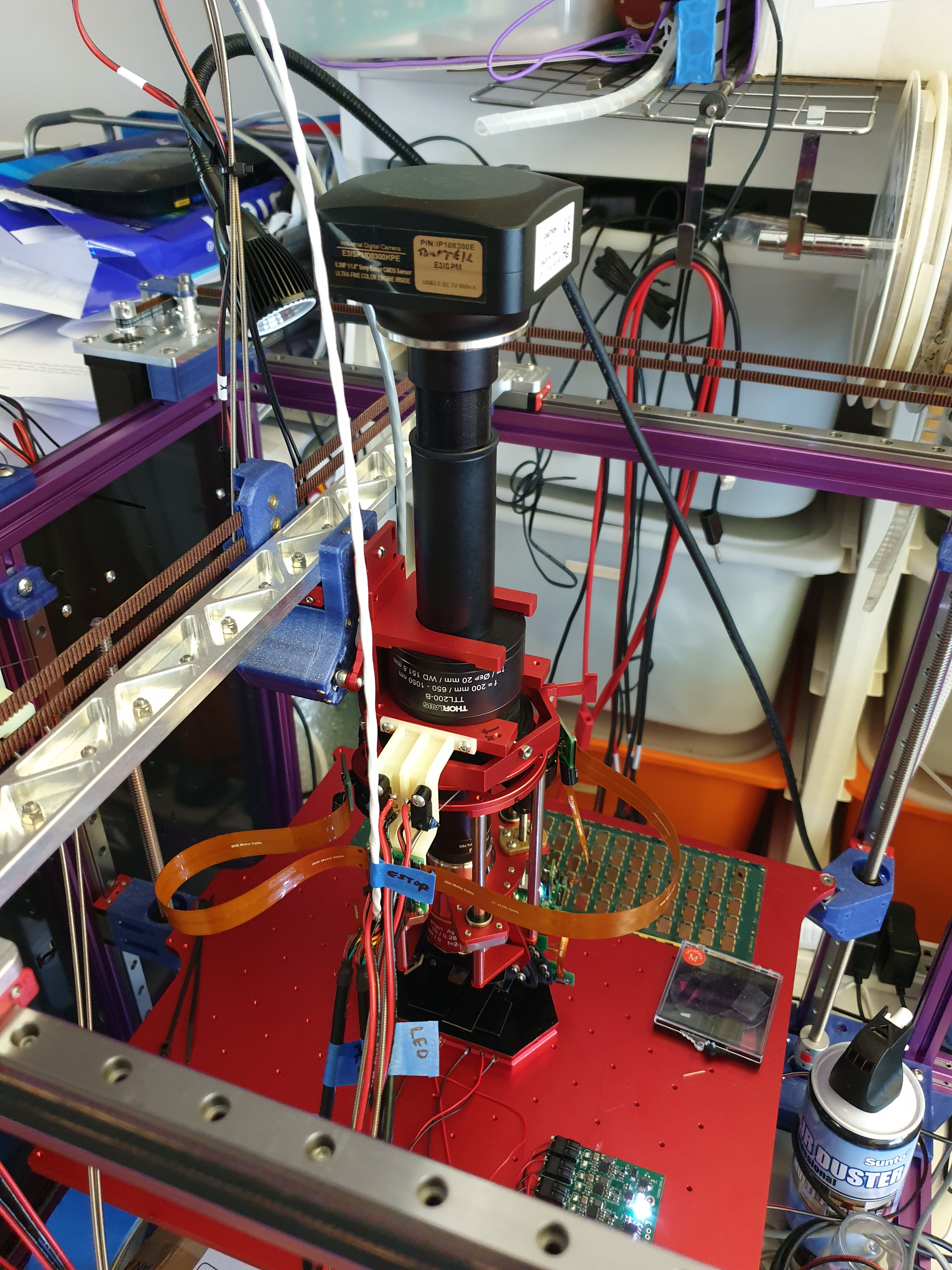
Above is the IRIS machine that I’ve constructed. There’s rather a lot occurring right here – however principally, it’s an IR digicam hooked up to a microscope, a nanometer-resolution focusing mechanism, and a pair of 1050nm gentle sources which have constantly adjustable azimuth and zenith. This microscope meeting is mounted in a Jubilee movement platform. The Jubilee is open source, and was designed by Joshua Vasquez of Prof. Nadya Peek‘s Machine Agency group. I acquired it as a equipment from Filastruder. The bottom movement platform is able to 10 micron steps, and incorporates a kinematically coupled Z-bed with three unbiased actuators, permitting me to dynamically compensate for planarity points within the pattern present process imaging.
Above is a brief video loop exhibiting the core mechanics in motion. The bizarre factor on the underside with the crimson and black wires popping out of it’s the kinematically coupled nanometer-resolution wonderful focus stage; its motions are too small to be picked up by the digicam.
An specific objective of this challenge is to open supply all of IRIS, in order that anybody can replicate the imaging system. Democratizing chip verification is necessary as a result of a reputable risk of being caught reduces the inducement of adversaries to deploy costly Trojan-implantation capabilities.
With little worry of being caught, there’s a payoff even when an adversary has to plow tens of thousands and thousands of {dollars} right into a functionality for planting chip-level {hardware} Trojans in high-value targets. Nevertheless, if chip inspection gear can bought within the ballpark of lots of to maybe 1000’s of {dollars}, and greater than a handful of customers are identified to routinely examine chips, the trail to payoff for an adversary earlier than they’re caught turns into murky. On this case, a rational adversary could also be deterred from focusing on an IRIS-enabled design, as a substitute reserving their capabilities just for the chips which can be troublesome to examine.
Other than that, I’ll be straight with you – an enormous motivation for IRIS is just because I’m curious, and I wish to look inside chips and see how they’re constructed (and it’s form of enjoyable and surprisingly satisfying to construct robots). I haven’t been disenchanted with what I’ve seen to date – I’ve to cease myself from losing evenings searching by the development of chips. I’ve achieved a little bit of chip design prior to now, and it’s fascinating to see the variety of methods and new developments in chip designs. I’m excited to share this sense of marvel with kindred spirits!
Given the amount of fabric to cowl, I’m going to interrupt the documentation up right into a sequence of weblog posts that go into the methodology used to construct the machine, in addition to particulars about each customized part, and the design choices that went into them. I’ll additionally summarize the standing of the evaluation software program that accompanies the system – so keep tuned for extra posts!
Nevertheless, for those who’re impatient and don’t wish to watch for the documentation, you possibly can already browse the supply recordsdata for the microscope, control software, stitching software, and layout extraction software.
Lastly, an enormous shout-out to NLnet and the European Fee. NLnet’s NGI0 Entrust fund, established with help from the European Commission’s Next Generation Internet Program, are instrumental in facilitating my work on IRIS. Additionally an enormous shout-out to my Github Sponsors for his or her unbelievable generosity and month-to-month help. Due to all these donors, I’m capable of preserve IRIS 100% open supply and freed from conflicts of curiosity with industrial traders.

You possibly can leave a response, or trackback from your individual web site.